- 您现在的位置:买卖IC网 > Sheet目录3884 > PIC18F448T-I/L (Microchip Technology)IC MCU FLASH 8KX16 W/CAN 44-PLCC
PIC18FXX8
DS41159E-page 10
2006 Microchip Technology Inc.
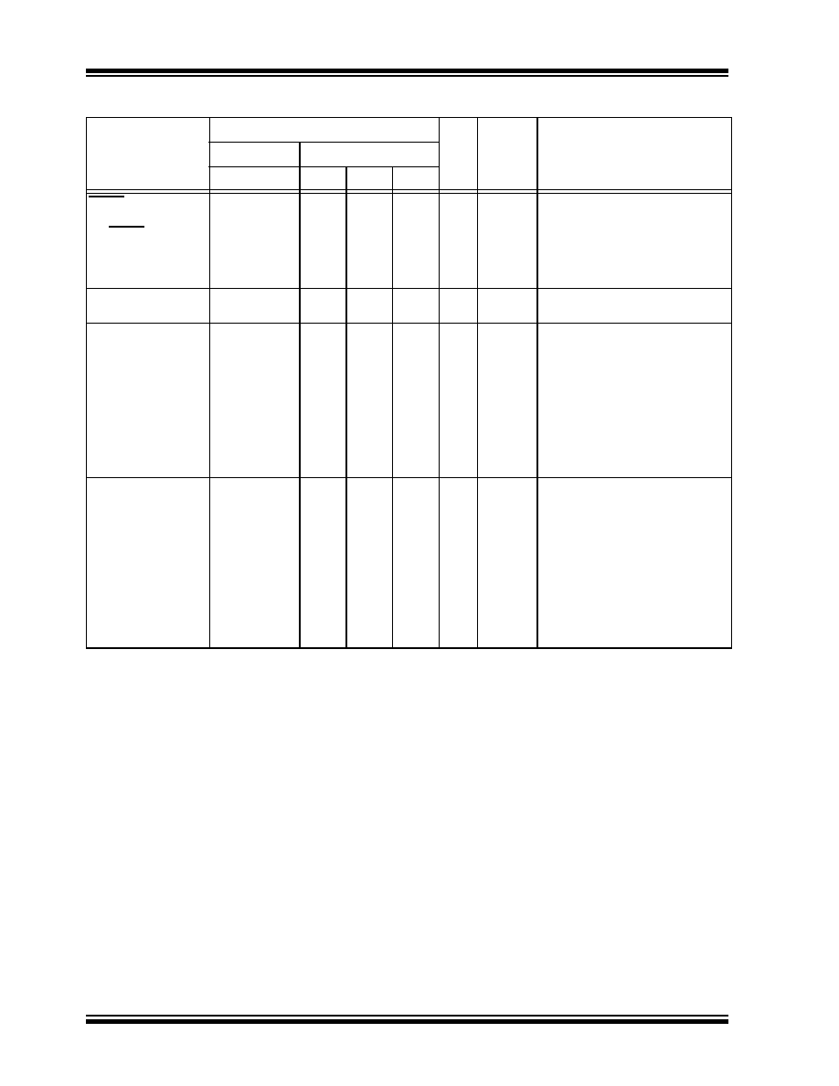
TABLE 1-2:
PIC18FXX8 PINOUT I/O DESCRIPTIONS
Pin Name
Pin Number
Pin
Type
Buffer
Type
Description
PIC18F248/258
PIC18F448/458
SPDIP, SOIC
PDIP
TQFP
PLCC
MCLR/VPP
MCLR
VPP
11
18
2
I
P
ST
—
Master Clear (input) or
programming voltage (output).
Master Clear (Reset) input.
This pin is an active low Reset
to the device.
Programming voltage input.
NC
—
12, 13,
33, 34
1, 17,
28, 40
—
These pins should be left
unconnected.
OSC1/CLKI
OSC1
CLKI
9
133014
I
CMOS/ST
CMOS
Oscillator crystal or external clock
input.
Oscillator crystal input or
external clock source input. ST
buffer when configured in RC
mode; otherwise, CMOS.
External clock source input.
Always associated with pin
function OSC1 (see OSC1/
CLKI, OSC2/CLKO pins).
OSC2/CLKO/RA6
OSC2
CLKO
RA6
10
14
31
15
O
I/O
—
TTL
Oscillator crystal or clock output.
Oscillator crystal output.
Connects to crystal or
resonator in Crystal Oscillator
mode.
In RC mode, OSC2 pin outputs
CLKO, which has 1/4 the
frequency of OSC1 and
denotes the instruction cycle
rate.
General purpose I/O pin.
Legend: TTL = TTL compatible input
CMOS = CMOS compatible input or output
ST
= Schmitt Trigger input with CMOS levels
Analog = Analog input
I
= Input
O
= Output
P
= Power
OD
= Open-Drain (no P diode to VDD)
发布紧急采购,3分钟左右您将得到回复。
相关PDF资料
PIC18LF448T-I/L
IC MCU FLASH 8KX16 LV CAN 44PLCC
PIC18LF458T-I/L
IC MCU FLSH 16KX16 LV CAN 44PLCC
PIC16F627-04E/P
IC MCU FLASH 1KX14 18-DIP
PIC16F627-20E/P
IC MCU FLASH 1KX14 18-DIP
PIC16C54C-20I/P
IC MCU OTP 512X12 18DIP
PIC16F627T-04E/SO
IC MCU FLASH 1KX14 18-SOIC
PIC18LF448-I/L
IC PIC MCU FLASH 8KX16 44PLCC
PIC18F448-E/P
IC MCU FLASH 8KX16 W/CAN 40-DIP
相关代理商/技术参数
PIC18F448T-I/PT
功能描述:8位微控制器 -MCU 16KB 768 RAM 34 I/O RoHS:否 制造商:Silicon Labs 核心:8051 处理器系列:C8051F39x 数据总线宽度:8 bit 最大时钟频率:50 MHz 程序存储器大小:16 KB 数据 RAM 大小:1 KB 片上 ADC:Yes 工作电源电压:1.8 V to 3.6 V 工作温度范围:- 40 C to + 105 C 封装 / 箱体:QFN-20 安装风格:SMD/SMT
PIC18F44J10-I/ML
功能描述:8位微控制器 -MCU 16 KB FL 1024 RAM RoHS:否 制造商:Silicon Labs 核心:8051 处理器系列:C8051F39x 数据总线宽度:8 bit 最大时钟频率:50 MHz 程序存储器大小:16 KB 数据 RAM 大小:1 KB 片上 ADC:Yes 工作电源电压:1.8 V to 3.6 V 工作温度范围:- 40 C to + 105 C 封装 / 箱体:QFN-20 安装风格:SMD/SMT
PIC18F44J10-I/P
功能描述:8位微控制器 -MCU 16 KB FL 1024 RAM RoHS:否 制造商:Silicon Labs 核心:8051 处理器系列:C8051F39x 数据总线宽度:8 bit 最大时钟频率:50 MHz 程序存储器大小:16 KB 数据 RAM 大小:1 KB 片上 ADC:Yes 工作电源电压:1.8 V to 3.6 V 工作温度范围:- 40 C to + 105 C 封装 / 箱体:QFN-20 安装风格:SMD/SMT
PIC18F44J10-I/PT
功能描述:8位微控制器 -MCU 16 KB FL 1 KB RAM RoHS:否 制造商:Silicon Labs 核心:8051 处理器系列:C8051F39x 数据总线宽度:8 bit 最大时钟频率:50 MHz 程序存储器大小:16 KB 数据 RAM 大小:1 KB 片上 ADC:Yes 工作电源电压:1.8 V to 3.6 V 工作温度范围:- 40 C to + 105 C 封装 / 箱体:QFN-20 安装风格:SMD/SMT
PIC18F44J10T-I/ML
功能描述:8位微控制器 -MCU 16 KB FL 1024 RAM RoHS:否 制造商:Silicon Labs 核心:8051 处理器系列:C8051F39x 数据总线宽度:8 bit 最大时钟频率:50 MHz 程序存储器大小:16 KB 数据 RAM 大小:1 KB 片上 ADC:Yes 工作电源电压:1.8 V to 3.6 V 工作温度范围:- 40 C to + 105 C 封装 / 箱体:QFN-20 安装风格:SMD/SMT
PIC18F44J10T-I/PT
功能描述:8位微控制器 -MCU 16 KB FL 1024 RAM RoHS:否 制造商:Silicon Labs 核心:8051 处理器系列:C8051F39x 数据总线宽度:8 bit 最大时钟频率:50 MHz 程序存储器大小:16 KB 数据 RAM 大小:1 KB 片上 ADC:Yes 工作电源电压:1.8 V to 3.6 V 工作温度范围:- 40 C to + 105 C 封装 / 箱体:QFN-20 安装风格:SMD/SMT
PIC18F44J11-I/ML
功能描述:8位微控制器 -MCU 16KB Flash 4KBRAM 12MIPS nanoWatt RoHS:否 制造商:Silicon Labs 核心:8051 处理器系列:C8051F39x 数据总线宽度:8 bit 最大时钟频率:50 MHz 程序存储器大小:16 KB 数据 RAM 大小:1 KB 片上 ADC:Yes 工作电源电压:1.8 V to 3.6 V 工作温度范围:- 40 C to + 105 C 封装 / 箱体:QFN-20 安装风格:SMD/SMT
PIC18F44J11-I/PT
功能描述:8位微控制器 -MCU 16KB Flash 4KBRAM 12MIPS nanoWatt RoHS:否 制造商:Silicon Labs 核心:8051 处理器系列:C8051F39x 数据总线宽度:8 bit 最大时钟频率:50 MHz 程序存储器大小:16 KB 数据 RAM 大小:1 KB 片上 ADC:Yes 工作电源电压:1.8 V to 3.6 V 工作温度范围:- 40 C to + 105 C 封装 / 箱体:QFN-20 安装风格:SMD/SMT